- 您现在的位置:买卖IC网 > Sheet目录349 > PCA9550DP,118 (NXP Semiconductors)IC LED DRIVER BLINKER 8-TSSOP
NXP Semiconductors
PCA9550
2-bit I 2 C-bus LED driver with programmable blink rates
? Process issues, such as application of adhesive and ?ux, clinching of leads, board
transport, the solder wave parameters, and the time during which components are
exposed to the wave
? Solder bath speci?cations, including temperature and impurities
15.4 Re?ow soldering
Key characteristics in re?ow soldering are:
? Lead-free versus SnPb soldering; note that a lead-free re?ow process usually leads to
higher minimum peak temperatures (see Figure 26 ) than a SnPb process, thus
reducing the process window
? Solder paste printing issues including smearing, release, and adjusting the process
window for a mix of large and small components on one board
? Re?ow temperature pro?le; this pro?le includes preheat, re?ow (in which the board is
heated to the peak temperature) and cooling down. It is imperative that the peak
temperature is high enough for the solder to make reliable solder joints (a solder paste
characteristic). In addition, the peak temperature must be low enough that the
packages and/or boards are not damaged. The peak temperature of the package
depends on package thickness and volume and is classi?ed in accordance with
Table 15 and 16
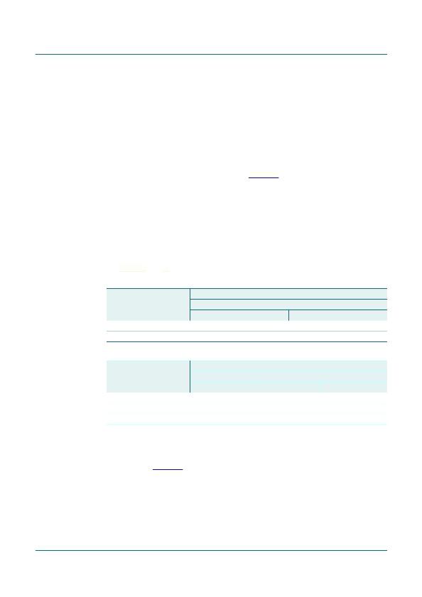
Table 15.
SnPb eutectic process (from J-STD-020C)
Package thickness (mm)
Package re?ow temperature ( ° C)
Volume (mm 3 )
< 350
≥ 350
< 2.5
≥ 2.5
Table 16.
235
220
Lead-free process (from J-STD-020C)
220
220
Package thickness (mm)
Package re?ow temperature ( ° C)
Volume (mm 3 )
< 350
350 to 2000
> 2000
< 1.6
1.6 to 2.5
> 2.5
260
260
250
260
250
245
260
245
245
Moisture sensitivity precautions, as indicated on the packing, must be respected at all
times.
Studies have shown that small packages reach higher temperatures during re?ow
soldering, see Figure 26 .
PCA9550_5
? NXP B.V. 2008. All rights reserved.
Product data sheet
Rev. 05 — 13 October 2008
22 of 26
发布紧急采购,3分钟左右您将得到回复。
相关PDF资料
PCA9551BS,118
IC LED DRIVER BLINKER 16-HVQFN
PCA9552D,118
IC LED DRIVER BLINKER 24-SOIC
PCA9553DP/01,118
IC LED DRIVER LINEAR 8-TSSOP
PCA9624PW,118
IC LED DRIVER RGBA 24-TSSOP
PCA9625D/S911,518
IC LED DRIVER RGBA 32-SOIC
PCA9626BS,518
IC LED DRIVER RGBA 48HVQFN
PCA9632DP2,118
IC LED DRIVER RGBA 10-TSSOP
PCA9633BS,118
IC LED DRIVER RGBA 16-HVQFN
相关代理商/技术参数
PCA9550DP,118-CUT TAPE
制造商:NXP 功能描述:PCA9550 Series 2-Bit I2C-Bus LED Driver w/ Programmable Blink Rates - TSSOP - 8
PCA9550DP118
制造商:Rochester Electronics LLC 功能描述: 制造商:NXP 功能描述: 制造商:NXP Semiconductors 功能描述:
PCA9550DP-T
功能描述:LED照明驱动器 2-BIT I2C FM OD LED BLK RST RoHS:否 制造商:STMicroelectronics 输入电压:11.5 V to 23 V 工作频率: 最大电源电流:1.7 mA 输出电流: 最大工作温度: 安装风格:SMD/SMT 封装 / 箱体:SO-16N
PCA9550TK
制造商:PHILIPS 制造商全称:NXP Semiconductors 功能描述:2-bit I2C-bus LED driver with programmable blink rates
PCA9551
制造商:PHILIPS 制造商全称:NXP Semiconductors 功能描述:8-bit I2C-bus LED driver with programmable blink rates
PCA9551BS
制造商:PHILIPS 制造商全称:NXP Semiconductors 功能描述:8-bit I2C-bus LED driver with programmable blink rates
PCA9551BS,118
功能描述:LED照明驱动器 8-BIT I2C FM OD LED RoHS:否 制造商:STMicroelectronics 输入电压:11.5 V to 23 V 工作频率: 最大电源电流:1.7 mA 输出电流: 最大工作温度: 安装风格:SMD/SMT 封装 / 箱体:SO-16N
PCA9551BS118
制造商:Rochester Electronics LLC 功能描述: 制造商:NXP 功能描述: 制造商:NXP Semiconductors 功能描述:
